


Originally published on 3M News Center
NORTHAMPTON, MA / ACCESS Newswire / October 30, 2025 / 3M
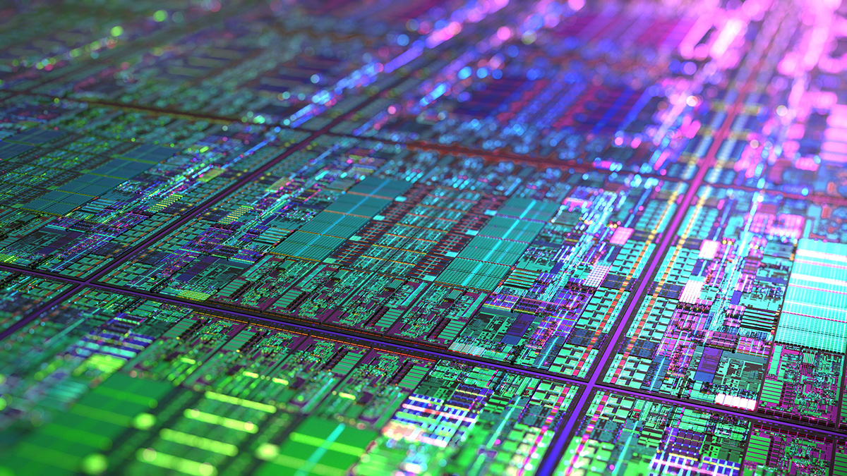
From smartphones to data centers, semiconductors sit at the core of modern life. Now, with the exponential growth in artificial intelligence (AI) applications, high-performance computing and advanced memory are driving a new wave of demand for semiconductor chips - and stretching the limits of traditional manufacturing processes in semiconductor fabrication facilities, also called "fabs."
Industry groups project global wafer-fabrication equipment spending will set new records in 2025 as manufacturers add capacity to support AI and advanced packaging, like those driven by the latest chip designs. In addition to industry-leading trends like chiplets, hybrid bonding, and 3D integration, technologies like silicon photonics and co-packaged optics (CPOs) will reshape how chips are interconnected, driving new requirements for yield, flatness, and thermal stability. Meeting these needs requires not just new tools, but also new materials that can improve efficiency, reduce waste, and shorten time-to-yield.
"3M collaborates and innovates with our customers and eco-system partners to push the boundaries of materials science to help them unlock new efficiencies across the fab," said Lung Lin, vice president of 3M Display and Electronics. "From cleaner, flatter surfaces for next-generation interconnects, to smarter thermal solutions, our innovations are designed to help improve process stability and deliver efficiency. And as new technologies like silicon photonics and co-packaged optics emerge, we're ready to help our customers integrate them with confidence."
Materials that enable efficiency across the fab
For decades, 3M has partnered with semiconductor manufacturers to deliver advanced materials that support cleaner processes, higher yields, and greater throughput. Today, our portfolio spans multiple stages of wafer manufacturing:
CMP materials (pads, and composite systems): Enable precise planarization - these polishing materials smooth each wafer layer so the next one can be built on a perfectly flat surface.
Pad conditioners: Maintain pad performance and uniformity - these pads act like "refreshening" tools to keep polishing pads effective, making sure that wafers are polished evenly.
Wafer support systems including bonding and protective tapes: Support wafer thinning, handling, and backside processing - these tapes hold wafers securely during processing, then the tapes remove easily
Heat-resistant tapes: Safeguards sensitive parts of the chip through soldering, molding, and high-temperature processing.
Each of these solutions reflects 3M's ability to apply deep expertise in abrasives, adhesives, and thermal management to some of the most complex manufacturing environments in the world.
Aligning with industry trends
Global shifts are reinforcing the need for advanced semiconductor materials:
AI and packaging growth: As AI chips get larger and pull in more memory, the connections between different parts of the chips need to be ultra-precise, requiring extremely flat, clean, and bondable wafer surfaces that fit and work together reliably.
3D integration and chiplets: Instead of just making chips smaller, manufacturers are stacking them and linking smaller chiplets together, driving new approaches to stacking and interconnecting. Materials that support precision bonding and stable wafer handling are increasingly critical.
Silicon photonics and co-packaged optics: Integrating optical and electronic components into the same package will redefine how chips communicate, and 3M can apply its expertise in bonding, thermal management, and precision handling as technology advances.
From wafer to workload
As the semiconductor industry scales to meet AI demand, efficiency gains at the fab level ripple outward. Materials that extend pad life, stabilize thermal performance, and enable reliable wafer handling not only save time and resources in production, they also help speed the availability of next-generation chips.
At the same time, AI's rapid adoption is fueling new energy demands downstream. The International Energy Agency projects that global data center electricity use could more than double by 2030, with AI noted as a leading driver. That's why 3M's broader energy solutions, including sensored cable accessories, and optical interconnects - complement our semiconductor offerings. Together, they support a more sustainable digital infrastructure, from the wafer fabrication to the data center.
3M is committed to advancing the semiconductor industry through materials innovation. By enabling efficiency, improving reliability, and supporting environmental goals, we help manufacturers meet the needs of today's AI-driven era-and prepare for the technologies still to come.
View additional multimedia and more ESG storytelling from 3M on 3blmedia.com.
Contact Info:
Spokesperson: 3M
Website: https://www.3blmedia.com/profiles/3m
Email: info@3blmedia.com
SOURCE: 3M
View the original press release on ACCESS Newswire:
https://www.accessnewswire.com/newsroom/en/business-and-professional-services/shaping-tomorrows-microchips-3m-materials-science-innovations-in-1093785
